
5. Why High-Performance Chillers Are Essential
ICP-MS is, at its core, a thermally governed measurement chain. Each stage — plasma generation, ion extraction, mass analysis, and detection — is sensitive to temperature, and thermal drift anywhere along the chain propagates into the analytical result. The following sections describe the engineering mechanisms by which temperature stability underpins performance.
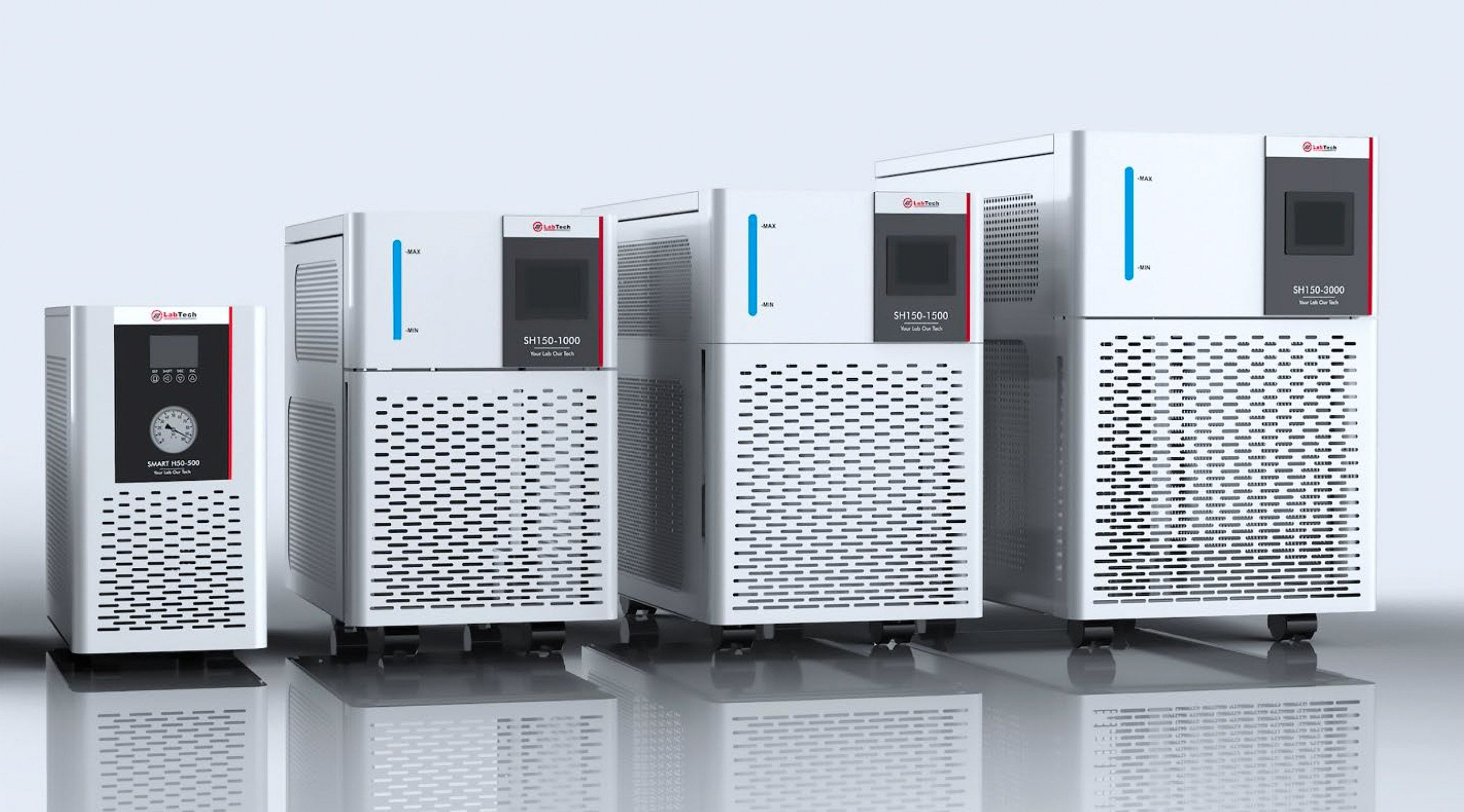
Facility cooling water and ambient air conditioning cannot meet the thermal requirements described above. House chilled water fluctuates with building load, may carry corrosive ions and particulates, and offers neither stability nor the cleanliness an ICP-MS demands. A dedicated recirculating laboratory chiller is therefore not an accessory but an integral subsystem of the instrument. Its essential characteristics are:
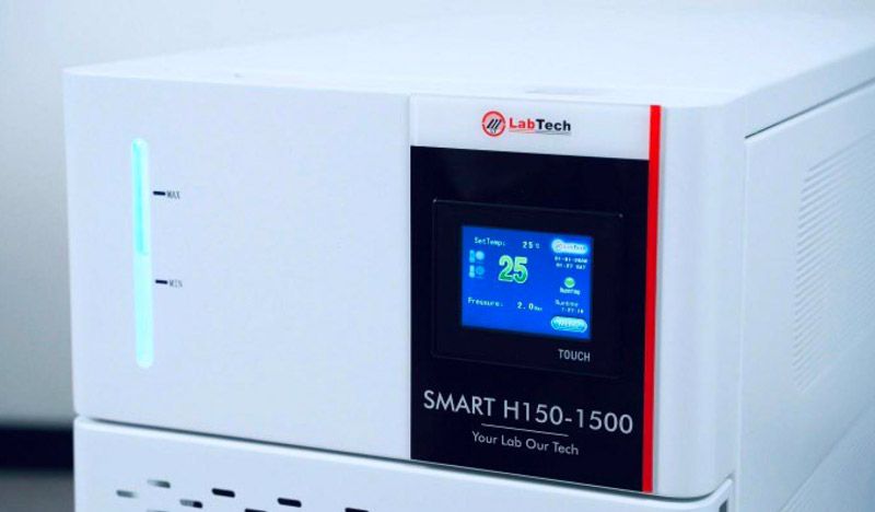
- Precise temperature stability (±0.1 °C or better). The cooling loop must hold setpoint to ±0.1 °C or better. Because plasma coupling, RF output, and detector gain all respond to fractions of a degree, anything loose allows measurable drift into the analytical result.
- Stable coolant flow rate. Heat removal depends on both temperature and flow. A stable, well-regulated coolant flow rate ensures the load coil, interface, and pumps receive constant cooling; flow surges or sag change component temperatures even when the setpoint is nominally held.
- Continuous 24/7 operation. Semiconductor analytical labs run around the clock. The chiller must sustain continuous operation 24/7 for years without performance degradation, since an unplanned chiller stoppage idles the ICP-MS and the QC pipeline that depends on it.
- High cooling capacity. The chiller must have sufficient cooling capacity to absorb the full thermal load of the RF generator, interface, and vacuum pumps simultaneously, with headroom for warm ambient conditions, so it never operates at its limit.
- Low vibration. Compressor and pump vibration can be coupled mechanically into the spray chamber, nebulizer, and ion optics, modulating signal. A low-vibration design — through compressor isolation and balanced pumps — protects measurement stability.
- Low maintenance requirements. Features such as accessible filters, sealed circuits, and robust components minimize maintenance and keep the chiller from becoming the limiting factor in instrument uptime.
- Long-term instrument protection. By holding the RF generator, cones, and pumps within their design temperature windows, the chiller reduces thermal stress and extends the service life of the most expensive ICP-MS components — delivering long-term instrument protection.
7. Conclusion
As semiconductor manufacturing advances to 2 nm and beyond, the tolerance for metallic contamination has collapsed to the ppt and ppq regime, and ICP-MS has become indispensable for the ultra-trace elemental analysis that protects wafer yield. Yet the sensitivity of ICP-MS is only half the story. That sensitivity is realized in practice only when the instrument operates in a thermally stable state, because plasma coupling, RF power, detector gain, vacuum integrity, interface behavior, and sample introduction are all governed by temperature. Thermal instability does not merely add noise, it introduces systematic drift that can masquerade as a real process signal or mask one, with direct consequences for yield decisions.
For this reason, a high-performance recirculating chiller delivering ±0.1 °C stability, regulated flow, ample capacity, corrosion-resistant construction, and reliable 24/7 operation is not a peripheral convenience but a core enabler of analytical performance. Investing in the right chiller maximizes accuracy and precision, reduces downtime and maintenance cost, extends the life of the ICP-MS's most expensive subsystems, and ultimately underpins the stringent quality requirements of advanced semiconductor fabrication. In the modern fab, exceptional thermal stability and exceptional analytical sensitivity are inseparable and the chiller is where that stability begins. LabTech's recirculating chillers are built for exactly this role, holding setpoint within ±0.1 °C with reliable, low-vibration 24/7 operation. Discover LabTech’s Water Chiller range.
Via Fatebenefratelli, 1/5
24010 - Sorisole (BG) - Italy
P.IVA: IT03242600165
Sitemap
Contact Us
Phone +39 035 576614